图书简介
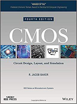
A revised guide to the theory and implementation of CMOS analog and digital IC design The fourth edition of CMOS: Circuit Design, Layout, and Simulation is an updated guide to the practical design of both analog and digital integrated circuits. The author-a noted expert on the topic-offers a contemporary review of a wide range of analog/digital circuit blocks including: phase-locked-loops, delta-sigma sensing circuits, voltage/current references, op-amps, the design of data converters, and switching power supplies. CMOS includes discussions that detail the trade-offs and considerations when designing at the transistor-level. The companion website contains numerous examples for many computer-aided design (CAD) tools. Using the website enables readers to recreate, modify, or simulate the design examples presented throughout the book. In addition, the author includes hundreds of end-of-chapter problems to enhance understanding of the content presented. This newly revised edition: * Provides in-depth coverage of both analog and digital transistor-level design techniques * Discusses the design of phase- and delay-locked loops, mixed-signal circuits, data converters, and circuit noise * Explores real-world process parameters, design rules, and layout examples * Contains a new chapter on Power Electronics Written for students in electrical and computer engineering and professionals in the field, the fourth edition of CMOS: Circuit Design, Layout, and Simulation is a practical guide to understanding analog and digital transistor-level design theory and techniques.
Preface xxxiii Chapter 1 Introduction to CMOS Design 1 1.1 The CMOS IC Design Process 1 1.1.1 Fabrication 2 1.2 CMOS Background 5 1.3 An Introduction to SPICE 8 Chapter 2 The Well 31 2.1 Patterning 32 2.1.1 Patterning the N-well 35 2.2 Laying Out the N-well 35 2.2.1 Design Rules for the N-well 36 2.3 Resistance Calculation 36 2.3.1 The N-well Resistor 38 2.4 The N-well/Substrate Diode 39 2.4.1 A Brief Introduction to PN Junction Physics 39 2.4.2 Depletion Layer Capacitance 42 2.4.3 Storage or Diffusion Capacitance 45 2.4.4 SPICE Modeling 46 2.5 The RC Delay through the N-well 48 2.6 Twin Well Processes 51 Chapter 3 The Metal Layers 59 3.1 The Bonding Pad 59 3.1.1 Laying Out the Pad I 60 3.2 Design and Layout Using the Metal Layers 63 3.2.1 Metal1 and Via1 63 3.2.2 Parasitics Associated with the Metal Layers 63 3.2.3 Current-Carrying Limitations 67 3.2.4 Design Rules for the Metal Layers 68 3.2.5 Contact Resistance 69 3.3 Crosstalk and Ground Bounce 70 3.3.1 Crosstalk 71 3.3.2 Ground Bounce 72 3.4 Layout Examples 74 3.4.1 Laying Out the Pad II 74 3.4.2 Laying Out Metal Test Structures 76 Chapter 4 The Active and Poly Layers 83 4.1 Layout Using the Active and Poly Layers 83 4.1.1 Process Flow 90 4.2 Connecting Wires to Poly and Active 93 4.3 Electrostatic Discharge (ESD) Protection 99 Chapter 5 Resistors, Capacitors, MOSFETs 107 5.1 Resistors 107 5.2 Capacitors 115 5.3 MOSFETs 118 5.4 Layout Examples 125 Chapter 6 MOSFET Operation 135 6.1 MOSFET Capacitance Overview/Review 136 6.2 The Threshold Voltage 139 6.3 IV Characteristics of MOSFETs 144 6.3.1 MOSFET Operation in the Triode Region 144 6.3.2 The Saturation Region 146 6.4 SPICE Modeling of the MOSFET 149 6.4.1 Some SPICE Simulation Examples 151 6.4.2 The Subthreshold Current 152 6.5 Short-Channel MOSFETs 154 6.5.1 MOSFET Scaling 155 6.5.2 Short-Channel Effects 156 6.5.3 SPICE Models for Our Short-Channel CMOS Process 157 Chapter 7 CMOS Fabrication by Jeff Jessing 165 7.1 CMOS Unit Processes 165 7.1.1 Wafer Manufacture 165 7.1.2 Thermal Oxidation 167 7.1.3 Doping Processes 168 7.1.4 Photolithography 170 7.1.5 Thin Film Removal 173 7.1.6 Thin Film Deposition 177 7.2 CMOS Process Integration 180 7.2.1 Frontend-of-the-Line Integration 182 7.2.2 Backend-of-the-Line Integration 196 7.3 Backend Processes 210 7.4 Advanced CMOS Process Integration 212 7.4.1 FinFETs 213 7.4.2 Dual Damascene Low-k/Cu Interconnects 216 7.5 Summary 219 Chapter 8 Electrical Noise: An Overview 221 8.1 Signals 221 8.1.1 Power and Energy 221 8.1.2 Power Spectral Density 223 8.2 Circuit Noise 226 8.2.1 Calculating and Modeling Circuit Noise 227 8.2.2 Thermal Noise 231 8.2.3 Signal-to-Noise Ratio 237 8.2.4 Shot Noise 247 8.2.5 Flicker Noise 251 8.2.6 Other Noise Sources 258 8.3 Discussion 260 8.3.1 Correlation 260 8.3.2 Noise and Feedback 264 8.3.3 Some Final Notes Concerning Notation 267 Chapter 9 Models for Analog Design 277 9.1 Long-Channel MOSFETs 277 9.1.1 The Square-Law Equations 279 9.1.2 Small Signal Models 286 9.1.3 Temperature Effects 300 9.2 Short-Channel MOSFETs 302 9.2.1 General Design (A Starting Point) 303 9.2.2 Specific Design (A Discussion) 306 9.3 MOSFET Noise Modeling 308 Chapter 10 Models for Digital Design 327 10.1 The Digital MOSFET Model 328 10.1.2 Process Characteristic Time Constant 331 10.1.3 Delay and Transition Times 333 10.1.4 General Digital Design 326 10.2 The MOSFET Pass Gate 326 10.2.1 Delay through a Pass Gate 338 10.2.2 Delay through Series-Connected PGs 340 10.3 A Final Comment Concerning Measurements 341 Chapter 11 The Inverter 347 11.1 DC Characteristics 347 11.2 Switching Characteristics 352 11.3 Layout of the Inverter 356 11.4 Sizing for Large Capacitive Loads 358 11.5 Other Inverter Configurations 364 Chapter 12 Static Logic Gates 369 12.1 DC Characteristics of the NAND and NOR Gates 369 12.1.1 DC Characteristics of the NAND Gate 369 12.1.2 DC Characteristics of the NOR Gate 372 12.2 Layout of the NAND and NOR Gates 373 12.3 Switching Characteristics 374 12.3.1 NAND Gate 375 12.3.2 Number of Inputs 378 12.4 Complex CMOS Logic Gates 379 Chapter 13 Clocked Circuits 389 13.1 The CMOS TG 389 13.2 Applications of the Transmission Gate 391 13.3 Latches and Flip-Flops 395 13.4 Examples 402 Chapter 14 Dynamic Logic Gates 411 14.1 Fundamentals of Dynamic Logic 411 14.1.1 Charge Leakage 411 14.1.2 Simulating Dynamic Circuits 414 14.1.3 Nonoverlapping Clock Generation 415 14.1.4 CMOS TG in Dynamic Circuits 416 14.2 Clocked CMOS Logic 417 Chapter 15 CMOS Layout Examples 425 15.1 Chip Layout 426 15.2 Layout Steps by Dean Moriarty 434 Chapter 16 Memory Circuits 445 16.1 Array Architectures 446 16.1.1 Sensing Basics 446 16.1.2 The Folded Array 452 16.1.3 Chip Organization 458 16.2 Peripheral Circuits 458 16.2.1 Sense Amplifier Design 458 16.2.2 Row/Column Decoders 467 16.2.3 Row Drivers 470 16.3 Memory Cells 471 16.3.1 The SRAM Cell 473 16.3.2 Read-Only Memory (ROM) 473 16.3.3 Floating Gate Memory 473 Chapter 17 Sensing Using Modulation 493 17.1 Qualitative Discussion 494 17.1.1 Examples of DSM 494 17.1.2 Using DSM for Sensing in Flash Memory 496 17.2 Sensing Resistive Memory 506 17.3 Sensing in CMOS Imagers 513 Chapter 18 Special Purpose CMOS Circuits 533 18.1 The Schmitt Trigger 533 18.1.1 Design of the Schmitt Trigger 534 18.1.2 Applications of the Schmitt Trigger 536 18.2 Multivibrator Circuits 538 18.2.1 The Monostable Multivibrator 539 18.2.2 The Astable Multivibrator 540 18.3 Input Buffers 541 18.3.1 Basic Circuits 541 18.3.2 Differential Circuits 543 18.3.3 DC Reference 547 18.3.4 Reducing Buffer Input Resistance 550 18.4 Charge Pumps (Voltage Generators) 551 18.4.1 Increasing the Output Voltage 553 18.4.2 Generating Higher Voltages: The Dickson Charge Pump 553 18.4.3 Example 556 Chapter 19 Digital Phase-Locked Loops 561 19.1 The Phase Detector 563 19.1.1 The XOR Phase Detector 563 19.1.2 The Phase Frequency Detector 567 19.2 The Voltage-Controlled Oscillator 570 19.2.1 The Current-Starved VCO 570 19.2.2 Source-Coupled VCOs 574 19.3 The Loop Filter 576 19.3.1 XOR DPLL 577 19.3.2 PFD DPLL 583 19.4 System Concerns 590 19.4.1 Clock Recovery from NRZ Data 593 19.5 Delay-Locked Loops 600 19.6 Some Examples 603 19.6.1 A 2 GHz DLL 603 19.6.2 A 1 Gbit/s Clock-Recovery Circuit 609 Chapter 20 Current Mirrors 621 20.1 The Basic Current Mirror 621 20.1.1 Long-Channel Design 622 20.1.2 Matching Currents in the Mirror 624 20.1.3 Biasing the Current Mirror 628 20.1.4 Short-Channel Design 634 20.1.5 Temperature Behavior 638 20.1.6 Biasing in the Subthreshold Region 642 20.2 Cascoding the Current Mirror 643 20.2.1 The Simple Cascode 643 20.2.2 Low-Voltage (Wide-Swing) Cascode 645 20.2.3 Wide-Swing, Short-Channel Design 648 20.2.4 Regulated Drain Current Mirror 651 20.3 Biasing Circuits 653 20.3.1 Long-Channel Biasing Circuits 653 20.3.2 Short-Channel Biasing Circuits 656 20.3.3 A Final Comment 657 Chapter 21 Amplifiers 671 21.1 Gate-Drain Connected Loads 671 21.1.1 Common-Source (CS) Amplifiers 671 21.1.2 The Source Follower (Common-Drain Amplifier) 683 21.1.3 Common Gate Amplifier 684 21.2 Current Source Loads 685 21.2.1 Common-Source Amplifier 685 21.2.2 The Cascode Amplifier 698 21.2.3 The Common-Gate Amplifier 702 21.2.4 The Source Follower (Common-Drain Amplifier) 702 21.3 The Push-Pull Amplifier 710 21.3.1 DC Operation and Biasing 711 21.3.2 Small-Signal Analysis 714 21.3.3 Distortion 716 Chapter 22 Differential Amplifiers 735 22.1 The Source-Coupled Pair 735 22.1.1 DC Operation 735 22.1.2 AC Operation 741 22.1.3 Common-Mode Rejection Ratio 745 22.1.4 Matching Considerations 746 22.1.5 Noise Performance 749 22.1.6 Slew-Rate Limitations 750 22.2 The Source Cross-Coupled Pair 750 22.2.1 Current Source Load 754 22.3 Cascode Loads (The Telescopic Diff-Amp) 756 22.4 Wide-Swing Differential Amplifiers 758 22.4.1 Current Differential Amplifier 760 22.4.2 Constant Transconductance Diff-Amp 760 Chapter 23 Voltage References 773 23.1 MOSFET-Resistor Voltage References 774 23.1.1 The Resistor-MOSFET Divider 774 23.1.2 The MOSFET-Only Voltage Divider 777 23.1.3 Self-Biased Voltage References 778 23.2 Parasitic Diode-Based References 784 23.2.1 Long-Channel BGR Design 787 23.2.2 Short-Channel BGR Design 795 Chapter 24 Operational Amplifiers I 803 24.1 The Two-Stage Op-Amp 804 24.2 An Op-Amp with Output Buffer 822 24.3 The Operational Transconductance Amplifier (OTA) 824 24.4 Gain-Enhancement 835 24.5 Some Examples and Discussions 839 Chapter 25 Dynamic Analog Circuits 857 25.1 The MOSFET Switch 857 25.1.1 Sample-and-Hold Circuits 861 25.2 Fully-Differential Circuits 864 25.2.1 A Fully-Differential Sample-and-Hold 866 25.3 Switched-Capacitor Circuits 869 25.3.1 Switched-Capacitor Integrator 871 25.4 Circuits 879 Chapter 26 Operational Amplifiers II 889 26.1 Biasing for Power and Speed 889 26.1.1 Device Characteristics 890 26.1.2 Biasing Circuit 891 26.2 Basic Concepts 892 26.3 Basic Op-Amp Design 900 26.4 Op-Amp Design Using Switched-Capacitor CMFB 920 Chapter 27 Nonlinear Analog Circuits 933 27.1 Basic CMOS Comparator Design 933 27.1.1 Characterizing the Comparator 939 27.1.2 Clocked Comparators 942 27.1.3 Input Buffers Revisited 943 27.2 Adaptive Biasing 943 27.3 Analog Multipliers 946 27.3.1 The Multiplying Quad 947 Chapter 28 Data Converter Fundamentals by Harry Li 955 28.1 Analog Versus Discrete Time Signals 955 28.2 Converting Analog Signals to Digital Signals 956 28.3 Sample-and-Hold (S/H) Characteristics 959 28.4 Digital-to-Analog Converter (DAC) Specifications 961 28.5 Analog-to-Digital Converter (ADC) Specifications 970 28.6 Mixed-Signal Layout Issues 979 Chapter 29 Data Converter Architectures by Harry Li 987 29.1 DAC Architectures 987 29.1.1 Digital Input Code 987 29.1.2 Resistor String 987 29.1.3 R-2R Ladder Networks 992 29.1.4 Current Steering 995 29.1.5 Charge-Scaling DACs 999 29.1.6 Cyclic DAC 1003 29.1.7 Pipeline DAC 1005 29.2 ADC Architectures 1006 29.2.1 Flash 1006 29.2.2 The Two-Step Flash ADC 1010 29.2.3 The Pipeline ADC 1014 29.2.4 Integrating ADCs 1018 29.2.5 The Successive Approximation ADC 1022 29.2.6 The Oversampling ADC 1027 Chapter 30 Implementing Data Converters 1043 30.1 R-2R Topologies for DACs 1043 30.1.1 The Current-Mode R-2R DAC 1044 30.1.2 The Voltage-Mode R-2R DAC 1045 30.1.3 A Wide-Swing Current-Mode R-2R DAC 1047 30.1.4 Topologies Without an Op-Amp 1057 30.2 Op-Amps in Data Converters 1063 30.2.1 Op-Amp Gain 1066 30.2.2 Op-Amp Unity Gain Frequency 1067 30.2.3 Op-Amp Offset 1067 30.3 Implementing ADCs 1070 30.3.1 Implementing the S/H 1071 30.3.2 The Cyclic ADC 1077 30.3.3 The Pipeline ADC 1084 Chapter 31 Feedback Amplifiers with Harry Li 1115 31.1 The Feedback Equation 1115 31.2 Properties of Negative Feedback on Amplifier Design 1117 31.2.1 Gain Desensitivity 1117 31.3 Recognizing Feedback Topologies 1120 31.3.1 Input Mixing 1121 31.3.2 Output Sampling 1121 31.3.3 The Feedback Network 1122 31.3.4 Calculating Open-Loop Parameters 1125 31.3.5 Calculating Closed-Loop Parameters 1127 31.4 The Voltage Amp (Series-Shunt Feedback) 1128 31.5 The Transimpedance Amp (Shunt-Shunt Feedback) 1134 31.5.1 Simple Feedback Using a Gate-Drain Resistor 1140 31.6 The Transconductance Amp (Series-Series Feedback) 1142 31.7 The Current Amplifier (Shunt-Series Feedback) 1146 31.8 Stability 1148 31.8.1 The Return Ratio 1151 31.9 Design Examples 1154 31.9.1 Voltage Amplifiers 1154 31.9.2 A Transimpedance Amplifier 1158 Chapter 32 Hysteretic Power Converters 1175 32.1 A Review of Power and Energy Basics 1176 32.1.1 Energy Storage in Inductors and Capacitors 1177 32.1.2 Energy Use in Transmitting Data 1180 32.1.3 Selection and use of Switches 1181 32.2 Switching Power Supplies: Some Examples 1189 32.2.1 The Buck SPS 1189 32.2.2 The Boost SPS 1196 32.2.3 The Flyback SPS 1200 32.2.4 Pulse Width Modulation: A Control Loop Example 1204 32.3 Hysteretic Control 1210 32.3.1 Topologies 1211 32.3.2 Examples 1212 Index 1219 About the Author 1235
Trade Policy 买家须知
- 关于产品:
- ● 正版保障:本网站隶属于中国国际图书贸易集团公司,确保所有图书都是100%正版。
- ● 环保纸张:进口图书大多使用的都是环保轻型张,颜色偏黄,重量比较轻。
- ● 毛边版:即书翻页的地方,故意做成了参差不齐的样子,一般为精装版,更具收藏价值。
关于退换货:- 由于预订产品的特殊性,采购订单正式发订后,买方不得无故取消全部或部分产品的订购。
- 由于进口图书的特殊性,发生以下情况的,请直接拒收货物,由快递返回:
- ● 外包装破损/发错货/少发货/图书外观破损/图书配件不全(例如:光盘等)
并请在工作日通过电话400-008-1110联系我们。
- 签收后,如发生以下情况,请在签收后的5个工作日内联系客服办理退换货:
- ● 缺页/错页/错印/脱线
关于发货时间:- 一般情况下:
- ●【现货】 下单后48小时内由北京(库房)发出快递。
- ●【预订】【预售】下单后国外发货,到货时间预计5-8周左右,店铺默认中通快递,如需顺丰快递邮费到付。
- ● 需要开具发票的客户,发货时间可能在上述基础上再延后1-2个工作日(紧急发票需求,请联系010-68433105/3213);
- ● 如遇其他特殊原因,对发货时间有影响的,我们会第一时间在网站公告,敬请留意。
关于到货时间:- 由于进口图书入境入库后,都是委托第三方快递发货,所以我们只能保证在规定时间内发出,但无法为您保证确切的到货时间。
- ● 主要城市一般2-4天
- ● 偏远地区一般4-7天
关于接听咨询电话的时间:- 010-68433105/3213正常接听咨询电话的时间为:周一至周五上午8:30~下午5:00,周六、日及法定节假日休息,将无法接听来电,敬请谅解。
- 其它时间您也可以通过邮件联系我们:customer@readgo.cn,工作日会优先处理。
关于快递:- ● 已付款订单:主要由中通、宅急送负责派送,订单进度查询请拨打010-68433105/3213。
本书暂无推荐
本书暂无推荐