图书简介
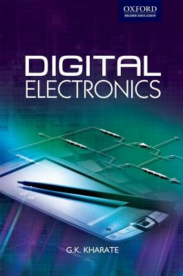
Digital Electronics is specially designed as a textbook for the undergraduate students of Electronics, Communciation, Computer Science, Electrical and Instrumentation Engineering for their introductory course on digital electronics or digital system and design.
I. LOGIC FAMILIES; 1.1 Introduction; 1.2 Logic Families; 1.3 Transistor as a Switch; 1.4 Characteristics of Digital ICs; 1.4.1. Speed of Operation; 1.4.2. Power Dissipation; 1.4.3. Figure of Merit; 1.4.4. Fan-out; 1.4.5. Fan-in; 1.4.6. Current and Voltage Parameters; 1.4.7. Noise Immunity; 1.4.8. Power Supply Requirements; 1.4.9. Operating Temperature; 1.5. Resistor - Transistor Logic (RTL); 1.6. Direct Coupled Transistor Logic (DCTC); 1.7. Diode - Transistor Logic (DTL); 1.8. Modified Diode - Transistor Logic; 1.9. Transistor - Transistor Logic (TTL); 1.9.1. TTL with passive pull-up; 1.9.2. TTL with totem - Pole output; 1.9.3. Wired and Connection; 1.9.4. TTL with open collector output; 1.9.5. Unconnected inputs of TTL; 1.9.6. Tri-StateTTL; 1.10. TTL Parameters; 1.11. Commonly used ICs of Standard TTL; 1.12. Improved TTL series; 1.12.1. Low Power and High Speed TTL; 1.12.2. Schottky TTL; 1.12.3. Lower Power Schottky TTL; 1.13. Comparison of TTL families; 1.14. Emitter Coupled Logic; 1.14.1. ECL Characteristics; 1.15. Integrated Injection Logic (I2L); 1.15.1. I2L Inverter; 1.15.2. I2L Nandgate; 1.15.3. I2L Nor gate; 1.16. MOSFET Logic; 1.17. NMOS; 1.17.1. MNOS Inverter; 1.17.2. NMOS NAND gate; 1.17.3. NMOS NOR gate; 1.17.4. Fan-out; 1.17.5. Propagation delay time; 1.17.6. Power dissipation; 1.18. CMOS; 1.18.1. CMOS inverter; 1.18.2. CMOS Nand gate; 1.18.3. CMOS NOR gate; 1.18.4. Characteristics of CMOS; 1.18.5. Buffered and Unbuffered gates; 1.18.6. Transmission gates; 1.18.7. Open drain outputs; 1.18.8. High impedance outputs; 1.18.9. Specifications and Standards; 1.19. Comparison of CMOS and TTL Families; 1.20. Interfacing CMOS and TTL Devices; 1.20.1. TTL Driving CMOS; 1.20.2. CMOS Driving TTL; 1.21. Interfacing of ECL and TTL devices; 1.21.1. TTL driving ECL; 1.21.2. ECL driving TTL; 1.22. Key terms & definitions; 1.23. Summary; 1.24. Exercise; 2. NUMBER SYSTEMS AND CODES; 2.1. Introduction; 2.2. Number Systems; 2.3. Interconversion of Numbers; 2.3.1. Binary to Decimal Conversion; 2.3.2. Decimal to Binary Conversion; 2.3.3. Octal to Decimal Conversion; 2.3.4. Decimal to Octal Conversion; 2.3.5. Octal to Binary Conversion; 2.3.6. Binary to Octal Conversion; 2.3.7. Hexadecimal to Decimal Conversion; 2.3.8. Decimal to Hexadecimal Conversion; 2.3.9. Hexadecimal to Binary Conversion; 2.3.10. Binary to Hexadecimal Conversion; 2.4. Signed Binary Number; 2.4.1. Sign-Magnitude Representation; 2.4.2. 1’s Complement Representation; 2.4.3. 2’s Complement Representation; 2.5. Floating Point Representation of Number; 2.6. Binary Arithmetic; 2.6.1. Binary Addition; 2.6.2. Binary Substraction; 2.6.3. Binary Multiplication; 2.6.4. Binary Division; 2.7. Complement Binary Arithmetic; 2.7.1. One’s (1’s) Compliment Arithmetic; 2.7.2. Two’s (2’s) Compliment Arithmetic; 2.8. Arithmetic Overflow; 2.9. Codes; 2.9.1. Classification of Codes; 2.9.2. BINARY Coded Decimal Code (BCD CODE); 2.9.2.1. BCD Arithmetic; 2.9.3. 2-4-2-1 Code; 2.9.4. Four-Bit BCD Codes; 2.9.5. Five Bit BCD Codes; 2.9.6. Biquinary Code; 2.9.7. Excess-3 Code; 2.9.8. Gray Code; 2.9.8.1. Binary to Gray Code Conversion; 2.9.8.2. Gray to Binary Code Conversion; 2.9.9. Seven Segment Code; 2.9.10. Alphanumeric Codes; 2.9.10.1. ASCII Code; 2.9.10.2. EBCDIC Code; 2.9.11. Error Detecting Codes; 2.9.11.1. Parity Codes; 2.9.11.2. Block Parity Codes; 2.9.12. Error Correcting Codes; 2.9.12.1. Linear Block Code; 2.9.12.2. Hamming Code; 2.10. Solved Examples; 2.11. Summary; 2.12. Exercises; 2.13. Problems; 2.14. Objective Type Questions; 3:BOOLEAN ALGEBRA AND LOGIC GATES; 3.1. Introduction; 3.2. Boolean Algebra; 3.2.1. Principal of Logic Circuits; 3.2.2. Boolean Constants, Variables and functions; 3.2.3. Basic laws of Boolean Algebra; 3.2.4. Boolean Theorems; 3.3. Overview of Logic Circuit; 3.4. Demorgan’s Theorems; 3.5. Standard Representation for logical functions; 3.5.1. Sum of products from; 3.5.2. Products of Sums; 3.6. Minterm and Maxterm; 3.7. Simplification of Boolean expression; 3.7.1. Algebraic method; 3.7.2. Karnaugh Map Simplification; 3.7.2.1. Representation of k-map; 3.7.2.2. Representation of truth table on K-map; 3.7.2.3. Representation of sum of products of K-map; 3.7.2.4. Representation of product of sum on K-map; 3.7.2.5 .Grouping the adjacent cells; 3.8. Simplification of sum of product expression; 3.9. Simplification of product of sums expression; 3.10. Don’t Care Condition; 3.11. Five and Six Variable K-map; 3.12. Quine McCluskey method; 3.13 Summary; 3.14.Exercise; 3.15 Objective Type Questions; 4: Combinational Logic Circuit; 4.1. Introduction; 4.2. Design Procedure for Combinational Logic Circuit; 4.2.1; Examples of Combinational Logic Circuit; 4.3. Adders; 4.3.1. Half adder; 4.3.2. Full adder; 4.3.3. N-Bit Parallel Adder; 4.3.4. Carry Look Ahead Adder; 4.3.5 IC 74LS83; 4.4. Subtractor; 4.4.1. Half subtractor; 4.4.2. Full subtractor; 4.4.3. N-Bit Parallel subtractor; 4.4.4.Four Bit subtractor Using Adder; 4.4.4.1; 1’s Complement Subtraction; 4.4.4.2 1’s Complement Subtraction; 4.5. BCD Adder; 4.6. BCD Subtractor; 4.6.1.9’s complement; 4.6.2.9’s complement subtraction; 4.6.3.10’scomplement; 4.6.4.10’s complement subtraction; 4.7. Arithmetic Logic Unit (ALU); 4.8. Comparator; 4.8.1 IC 7485 [4 Bit-Comparator]; 4.9. Parity generator; 4.9.1. Even parity generator; 4.9.2; Odd parity generator; 4.10. Parity checker; 4.10.1. Even parity checker; 4.10.2 Odd parity checker; 4.11 Parity generator/checker (IC74180); 4.12 Multiplexer; 4.12.1. Multiplexer Tree; 4.12.2. Multiplexer Applications; 4.13. Demultiplexer; 4.13.1. Demultiplexer Tree; 4.13.2. Demultiplexer Applications; 4.14. Code Converters; 4.14.1. Binary to BCD Converter; 4.14.2. BCD to Binary converter; 4.14.3. BCD to Excess - 3; 4.14.4. Excess - 3 to BCD Code Converter; 4.14.5. Binary to Gray Code Converter; 4.14.6. Gray to Binary Code Converter; 4.14.7. BCD to Seven-Segment code converter; 4.14.8. BCD to Seven-Segment display decoder/Driver; 4.14.9. Basic connection for driving 7-segment displays; 4.12.10..ICs of Seven-segment Driver/Decoder; 4.15. PIN diagrams of ICs; 4.16. Key terms and definitions; 4.17. Exercise; 4.18. Objective Type Questions; 5. SEQUENTIAL LOGIC; 5.1. Introduction; 5.2. One bit Memory Cell; 5.2.1. One bit Memory Cell using Transistors; 5.2.2. One bit Memory Cell using NAND gates; 5.2.3. One bit Memory Cell using NOR gates; 5.3. Clocked S.R. Flip-flop; 5.3.1. Preset and Clear inputs; 5.4. J-K Flip-Flop; 5.4.1. Race-Around condition; 5.4.2. Master-Slave j-K Flip-Flop; 5.5. D Flip-Flop; 5.6. T Flip-Flop; 5.7. Edge Triggered Flip-Flop; 5.8. Characterstics of Flip-Flop; 5.8.1. Propagation Delay (tp); 5.8.2. Set-up time (tg); 5.8.3. Hold-up time (tn); 5.8.4. Maximum check frequency (Fmax); 5.8.5. Asynchronous Active Pulse Width; 5.8.6. Clock high pulse time and low pulse time; 5.9. Flip-Flop Conversion; 5.9.1. S-R. Flip-Flop to T Flip-Flop; 5.9.2. S-R. Flip-Flop to D Flip-Flop; 5.9.3. S-R. Flip-Flop to J.K. Flip-Flop; 5.9.4. T Flip-Flop to D Flip-Flop; 5.9.5. D Flip-Flop to T Flip-Flop; 5.9.6. J-K. Flip-Flop to T Flip-Flop; 5.9.7.J-K. Flip-Flop to D Flip-Flop; 5.10Application of Flip-Flops; 5.10.1. Bounce Elimination Switch; 5.10.2. Registers; 5.10.3Counters; 5.10.4Random Access Memory; 5.11. Sequential Logic Design (Introduction); 5.12. Registers and Shift registers; 5.12.1Serial in serial out shift register; 5.12.2. Serial In parallel out shift register; 5.12.3Parallel in serial out shift register; 5.12.4. Parallel In Parallel out shift register; 5.12.5.Bi-directional shift register; 5.12.6. Universal register; 5.13. Applications of Shift register; 5.13.1. Serial to parallel converter; 5.13.2. Parallel to serial converter; 5.13.3. Ring counter; 5.13.4. Johnson counter and Twisted Ring counter; 5.13.5. Sequence generator; 5.13.6. Sequence detector; 5.14. Commonly used ICs for Shift register; 5.15.Ripple counter; 5.15.1. Up/Down Asynchronous counter; 5.15.2. Modulus ’M’ Asynchronous counter; 5.15.3. Commonly used ICs for Asynchronous counter; 5.16. Synchronous counter; 5.17. Flip-Flop Excitation table; 5.17.1. Excitation table of R-S flip-flop; 5.17.2. Excitation table of J-K flip-flop; 5.17.3. Excitation table of T flip-flop; 5.17.4. Excitation table of DT flip-flop; 5.18. Synchronous Counter Design; 5.19. UP/DOWN Counter; 5.19.1. Commonly used ICs for Synchronous Counter; 5.19.2; 74191; 5.19.3; 74192; 5.20. Clocked Sequential Circuit; 5.20.1; Moore Circuit; 5.20.2; Mealy Circuit; 5.21 Analysis of Clocked Sequential Circuit; 5.21.1; State Table; 5.21.2; State Diagram; 5.22 Design of Clocked Sequential Circuit; 5.22.1; State Table; 5.22.2; State Diagram; 5.22.3; State Reduction; 5.22.4; State Assignment; 5.23 Lockout Condition; 5.24 Sequence Generator; 5.25 Sequence Detector; 5.26. Summary; 5.27. Exercise; 5.28. Objective Type Questions; 6. ASYNCHRONOUS SEQUENTIAL CIRCUITS; 6.1 Introduction; 6.2 Design of Fundamental Mode Asynchronous Sequential Circuits; 6.2.1 Realization using D Flip-Flops; 6.2.2 Realization using JK Flip-Flops; 6.3 Design of Pulse Mode Asynchronous Sequential Circuits; 6.4 Incompletely Specified State Machines; 6.5 Problems in Asynchronous Circuits; 6.5.1 Cycles; 6.5.2 Races; 6.5.3 Hazards; 6.6 Design of Hazard Free Switching Circuits; 6.7 Summary; 6.8 Exercise; 6.9 Objective Type Questions; 7. ALGORITHMIC STATE MACHINES; 7.1. Introduction; 7.2. Algorithmic State Machines (ASM); 7.2.1. State Box; 7.2.2. Decision Box; 7.2.3. Conditional Box; 7.2.4. ASM block; 7.3. Realization of ASM charts; 7.3.1. Traditional Synthesis from an ASM chart; 7.3.2. Multiplexer Controller method; 7.4. Solved problems on ASM charts; 7.5. Register transfer language; 7.6. RTL Notations; 7.6.1. Register Transfer statements; 7.6.1.1Shift operation; 7.6.1.2. Rotate operation; 7.6.2. Logical Operation statement; 7.6.2.1. Inversion operation; 7.6.2.2. ANDing operation; 7.6.2.3. ORing operation; 7.6.3. Connection operation statement; 7.6.4. Branch statements; 7.6.4.1. Unconditional branch statement; 7.6.4.2Conditional branch statement; 7.6.5. Conditional transfer statement; 7.6.6. Count statement; 7.6.7. Declaration statement; 7.6.8. BUS connection statement; 7.7. Data Unit Construction from an RTL Description; 7.8. VHDL; 7.8.1. Entity - Architecture pair; 7.8.2. Entity Declaration.; 7.8.3. Architecture Body; 7.8.4. Structural Modeling; 7.8.4.1. Description of Full Adder Architecture; 7.8.4.2. Declarative part; 7.8.4.3. Statement part; 7.8.5. Data Flow Modeling; 7.8.5.1. WHEN - ELSE Statement; 7.8.5.2. With - Select Statement; 7.8.6. Behavioral Style of Modeling; 7.8.7. Sequential Statements used in behavioral modeling; 7.8.8. Mixed Style of Modeling; 7.8.9. Configurations; 7.8.9.1. Default Configurations; 7.8.9.2. Component Configuration; 7.8.10. Important Data Objects in VHDL; 7.8.10.1. Signal; 7.8.10.2. Variable; 7.8.10.3. Constant; 7.8.11. Important Data Types; 7.8.12, VHDL Operators; 7.8.13. VHDL Examples; 7.9. Summary; 7.11. Exercise; 8. PROGRAMMABLE LOGIC DEVICES; 8.1. Introduction; 8.2. Programmable Logic Array; 8.2.1 Internal diagram of PLA; 8.2.1.1, Input Buffer; 8.2.1.2. AND matrix; 8.2.1.3. OR matrix; 8.2.1.3. Invert/Non-invert matrix; 8.2.1.4. Output Buffer; 8.2.2. Combinational Logic Design using PLA; 8.2.3. Sequential Logic Design using PLA; 8.3. Programmable Array Logic; 8.3.1. Internal diagram of PAL; 8.3.2. Registered Output PALs; 8.3.3. Configurable PALs; 8.3.4. Combinational Logic design using PALs; 8.3.5. Sequential Logic design using PAL; 8.4. Generic Array Logic Devices (GALs); 8.4.1. Architecture of GAL 16V8; 8.5. Classification of PLDs; 8.6. Complex Programmable Logic Devices; 8.6.1. Xilinx XC 9500 CPLD family; 8.6.1.1. Internal Architecture; 8.6.1.2. Function - Block Architecture; 8.6.1.3. I/O Block of XC 9500; 8.6.1.4. Switch Matrix; 8.7. Field Programmable Gate Array; 8.7.1. Xilinx FPGA Architecture; 8.7.1.1. Configurable Logic Block; 8.7.1.2. Combinational Function Generator; 8.7.1.3. Flip-Flop; 8.7.1.4. Programmable Multiplexers; 8.7.1.5, Input-Output Block (IOB); 8.7.1.6. Switching Matrix Structure; 8.7.2. XC 4000 Series FPGA; 8.7.2.1. Configurable Logic Block of XC 400; 8.7.2.2. Input - Output Mock of XC 4000; 8.7.2.3. Programmable Interconnects; 8.8. Application Specific Integrated Circuits (ASICs); 8.8.1. Full Custom ASICs; 8. 8. 2. Semi-Custom ASICs; 8.8.2.1. Standard Cell Based ASICs; 8.8.2.2. Gate Array Based ASICs; 8.9. Solved Examples; 8.10. Summary; 8.11. Exercises; 9. CONVERTERS; 9.1. Introduction; 9.2. Basic Principle of D/A Converter; 9.2.1. Digital to Analog (D/A) converter circuits; 9.2.2. Digital to Analog Converter; 9.2.3. Specifications of D/A converter; Basic principle of Analog to Digital converter; 9.3.1Analog to Digital converter circuits; 9.3.2. Parallel Comparator Analog to Digital Converter (Flash Converter); 9.3.3 Successive-approximation A/D converter; 9.3.4. Dual slope A/D converter; 9.3.5. Specifications for Analog to Digital Converter; 9.4. D/A and A/D Converter ICs; 9.5. ADC 0809 (8 bit A/D converter); 9.6. ADC-7109 (12 Bit binary A/D converter); 9.7. DAC 0808 (8-bit D/A converter); 9.8. Solved Examples; 9.9. Summary; 9.10. Exercises; 10. SEMICONDUCTOR MEMORIES; 10.1. Introduction; 10.2. Memory Organization:; 10.3. Functional Diagram of Memory; 10.4. Memory Operations; 10.5. Expanding Memory Size:; 10.5.1. Expanding Word Size:; 10.5.2. Expanding word capacity:; 10.5.3. Expanding Of Word Size and Word Capacity:; 10.6. Characteristics of Memory Devices:; 10.7. Classification of Semiconducting Memories:; 10.8. Read and Write Memory:; 10.8.1. Static RAM; 10.8.2. Dynamic RAM:; 10.8.3. Comparison between SRAM and; 10.8.4. Commonly Used ICs for RAM:; 10.9. Read only memory (ROM); 10.10. Masked ROM:; 10.10.1. Programmable Read Only Memory (PROM): 10.10.2. Erasable Programmable Read Only Memory (EPROM):; 10.10.3. Electrical Erasable Programmable Read Only Memory (EEPROM):; 10.10.4. NVRAM; 10.11. Solved Examples; 10.12. Summary; 10.13. Exercises
Trade Policy 买家须知
- 关于产品:
- ● 正版保障:本网站隶属于中国国际图书贸易集团公司,确保所有图书都是100%正版。
- ● 环保纸张:进口图书大多使用的都是环保轻型张,颜色偏黄,重量比较轻。
- ● 毛边版:即书翻页的地方,故意做成了参差不齐的样子,一般为精装版,更具收藏价值。
关于退换货:- 由于预订产品的特殊性,采购订单正式发订后,买方不得无故取消全部或部分产品的订购。
- 由于进口图书的特殊性,发生以下情况的,请直接拒收货物,由快递返回:
- ● 外包装破损/发错货/少发货/图书外观破损/图书配件不全(例如:光盘等)
并请在工作日通过电话400-008-1110联系我们。
- 签收后,如发生以下情况,请在签收后的5个工作日内联系客服办理退换货:
- ● 缺页/错页/错印/脱线
关于发货时间:- 一般情况下:
- ●【现货】 下单后48小时内由北京(库房)发出快递。
- ●【预订】【预售】下单后国外发货,到货时间预计5-8周左右,店铺默认中通快递,如需顺丰快递邮费到付。
- ● 需要开具发票的客户,发货时间可能在上述基础上再延后1-2个工作日(紧急发票需求,请联系010-68433105/3213);
- ● 如遇其他特殊原因,对发货时间有影响的,我们会第一时间在网站公告,敬请留意。
关于到货时间:- 由于进口图书入境入库后,都是委托第三方快递发货,所以我们只能保证在规定时间内发出,但无法为您保证确切的到货时间。
- ● 主要城市一般2-4天
- ● 偏远地区一般4-7天
关于接听咨询电话的时间:- 010-68433105/3213正常接听咨询电话的时间为:周一至周五上午8:30~下午5:00,周六、日及法定节假日休息,将无法接听来电,敬请谅解。
- 其它时间您也可以通过邮件联系我们:customer@readgo.cn,工作日会优先处理。
关于快递:- ● 已付款订单:主要由中通、宅急送负责派送,订单进度查询请拨打010-68433105/3213。
本书暂无推荐
本书暂无推荐